


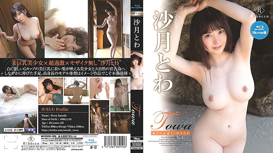
REBDB-309 日本AV 沙月的光芒将永远延续。 - 免费预告片中文字幕 srt。
下载 REBDB-309 字幕
 English Subtitles
 中文字幕
中文字幕
 日本語字幕
日本語字幕
 Subtitle Indonesia
 Deutsche Untertitel
 Sous-titres Français

关于 REBDB-309 日本AV视频
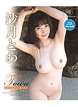
演员: 沙月とわ
片商: REbecca
导演: Chikara Sawamura
发布日期: 7月 19日 2018年
片长: 77 分钟
字幕价格: $115.5 每分钟 1.50 美元
字幕创建时间: 5 - 9 天
类型: 审查视频
国度: 日本
语言: 日文
字幕文件类型: .srt / .ssa
字幕文件大小: <77 KB (~5390 行翻译)
字幕文件名: h_346rebdb00309.srt
翻译: 人工翻译(非人工智能)
人数: 1人
视频质量: 320x240, 480x360, 852x480 (SD), 1280x720 (HD), 1920x1080 (HD)
拍摄地点: 在家
发行类型: 经常出现
演戏: 独唱演员
视频代码:
版权所有者: © 2018 DMM
视频质量
1080p (HD)3,479 MB
720p (HD)2,317 MB
576p1,742 MB
432p1,163 MB
288p598 MB
144p235 MB
常问问题
如何下载完整视频?
这部视频没有字幕。 你能为我创建它们吗?
自定义字幕订单如何收费?
字幕是什么格式?
如何播放带字幕的视频?

JAV Subtitled 为您最喜爱的日本AV视频提供最好的字幕和免费预告片。 浏览超过四十万个日本AV标题的集合,并立即下载每天发布的新字幕。
© 2019 - 2026 JAV Subtitled. 版权所有. (DMCA • 2257).
年龄限制:本网站仅面向年满18岁或以上的个人。内容可能包含仅适合成年人的材料,例如图像、视频和文本,不适合未成年人。您进入本网站即表示您已年满18岁,并接受以下条款和条件。本网站的所有者及其关联方不对您使用本网站可能产生的任何损害或法律后果负责,您需自行承担所有相关风险。
JAV Subtitled不在我们的任何服务器上托管任何视频或受版权保护的材料。 我们只是提供字幕服务,我们网站上显示的任何内容要么是公开的、免费的样本/预告片,要么是用户生成的内容。
年龄限制:本网站仅面向年满18岁或以上的个人。内容可能包含仅适合成年人的材料,例如图像、视频和文本,不适合未成年人。您进入本网站即表示您已年满18岁,并接受以下条款和条件。本网站的所有者及其关联方不对您使用本网站可能产生的任何损害或法律后果负责,您需自行承担所有相关风险。
JAV Subtitled不在我们的任何服务器上托管任何视频或受版权保护的材料。 我们只是提供字幕服务,我们网站上显示的任何内容要么是公开的、免费的样本/预告片,要么是用户生成的内容。
